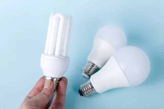
Light-emitting diodes have transformed modern illumination with a swiftness that few technological revolutions can match, yet the narrative that their development is complete could not be further from the truth. The fundamental physics governing photon emission from semiconductor junctions was settled decades ago, but the engineering reality of extracting every possible lumen from every watt of electricity remains an intensely active frontier. Recent research highlighted in September 2026 underscores a persistent truth: the next meaningful gains in LED performance will not emerge from cleverer driver circuits or smarter dimming protocols, but from painstaking advances at the atomic scale of materials science.
When we consider that lighting accounts for roughly fifteen percent of global electricity consumption, the stakes of incremental efficiency improvements become staggeringly clear. A single percentage point of efficacy gained across the world's installed base of solid-state lamps translates into terawatt-hours of annual energy savings and correspondingly significant reductions in carbon emissions. This is why the materials-science community continues to push against the physical limits of gallium nitride and its compound semiconductor relatives, seeking to close the gap between theoretical maximum performance and what can be reliably manufactured at scale. The LED revolution, in other words, is not over; it has simply moved from the domain of circuit architects into the laboratories of crystal growers and defect engineers.
Understanding why efficiency remains elusive requires a journey into the quantum mechanics of light emission, the crystallography of defect formation, and the thermodynamics of heat dissipation. Each layer of the LED structure presents its own optimization challenge, from the substrate upon which crystals are grown to the phosphor coatings that convert blue photons into warm white light. This analysis dissects those challenges with scientific rigor, presenting the mathematical frameworks that govern efficiency losses and exploring the novel material systems poised to redefine what solid-state lighting can achieve.
On This Page
- The Physics of Photon Generation and the Efficiency Ceiling
- Light Extraction and the Photon Escape Problem
- Thermal Management and the Efficiency-Temperature Nexus
- Materials Innovation Beyond Gallium Nitride
- Quantitative Analysis of LED Efficiency Limits
- The Path Forward and Remaining Challenges
- Conclusion and Research Outlook
The Physics of Photon Generation and the Efficiency Ceiling
At its heart, an LED converts electrical energy into photons through radiative recombination of electron-hole pairs within a semiconductor's active region. The efficiency of this conversion is governed by the ratio of radiative to non-radiative recombination pathways, a competition that materials scientists manipulate through careful bandgap engineering. When an electron falls from the conduction band to recombine with a hole in the valence band, the energy difference can either emerge as a photon or dissipate as heat through lattice vibrations known as phonons.
The theoretical maximum efficiency of this process, known as the internal quantum efficiency, approaches unity in ideal crystals. However, real devices suffer from a phenomenon called efficiency droop, where the quantum efficiency paradoxically decreases as current density increases. This droop effect, first identified in gallium nitride LEDs over a decade ago, remains one of the most studied and debated phenomena in solid-state lighting research.
Carrier Dynamics and the Auger Recombination Mechanism
The dominant explanation for efficiency droop centers on Auger recombination, a non-radiative process where the energy released by an electron-hole pair is transferred to another charge carrier rather than emitted as light. This three-particle interaction becomes increasingly probable at high carrier densities, precisely the operating regime where LEDs are driven for maximum light output. The Auger mechanism effectively steals photons that would otherwise contribute to useful illumination, converting them into kinetic energy that ultimately manifests as waste heat.
Quantifying the Auger coefficient requires sophisticated experimental techniques, including time-resolved photoluminescence and differential carrier lifetime measurements. Researchers have measured Auger coefficients in InGaN quantum wells ranging from ##[1 \times 10^{-30}##] to ##[1 \times 10^{-29} \text{ cm}^6\text{s}^{-1}##], values that vary significantly with indium composition and quantum well thickness. These measurements inform device models that predict the maximum achievable efficiency for a given epitaxial structure.
The mathematical treatment of Auger recombination begins with the rate equation describing carrier density decay, where the total recombination rate combines Shockley-Read-Hall, radiative, and Auger contributions. The differential equation governing carrier population under steady-state injection reveals how each mechanism scales differently with carrier concentration, explaining why droop emerges only at elevated current densities.
Recent theoretical work has challenged the simple band-to-band Auger model, proposing instead that indirect Auger processes mediated by phonons or alloy disorder play a dominant role in InGaN systems. These refined models better reproduce the temperature dependence of droop observed experimentally, suggesting that multiple microscopic pathways contribute to the efficiency loss. The debate remains active, with direct experimental evidence for specific Auger channels still elusive due to the difficulty of isolating individual recombination pathways.
Strategies to mitigate Auger losses include widening quantum wells to reduce carrier density at fixed current, engineering the band structure to suppress the Auger matrix element, and employing staggered or graded quantum well designs. Each approach involves trade-offs between carrier confinement, wavelength stability, and epitaxial complexity, requiring careful optimization through both simulation and growth experiments.
Defect-Mediated Non-Radiative Recombination
Beyond Auger processes, crystallographic defects provide alternative pathways for non-radiative recombination that plague real devices. Dislocations, point defects, and impurity complexes all introduce energy levels within the bandgap that can capture carriers and dissipate their energy as heat. The density of such defects depends critically on the substrate material and growth conditions, with lattice mismatch between the epitaxial layers and substrate being a primary source of threading dislocations.
Gallium nitride LEDs are typically grown on sapphire or silicon carbide substrates, neither of which matches the crystal lattice of GaN perfectly. The resulting strain is accommodated through the formation of misfit dislocations at the heterointerface, which thread upward through the device structure. Typical dislocation densities in commercial LEDs range from ##[10^7##] to ##[10^9 \text{ cm}^{-2}##], values that would be catastrophic for conventional semiconductor devices but are tolerable in LEDs due to the localized nature of carrier recombination.
The Shockley-Read-Hall theory provides the mathematical framework for understanding defect-mediated recombination, relating the recombination rate to the density and energy position of trap states. The SRH lifetime depends inversely on trap density and capture cross-section, with the strongest recombination occurring for traps near the intrinsic Fermi level. This sensitivity explains why trace impurities at parts-per-billion concentrations can measurably degrade LED efficiency.
Advanced characterization techniques, including cathodoluminescence mapping and deep-level transient spectroscopy, allow researchers to identify and quantify specific defect species within LED structures. These measurements reveal that efficiency losses correlate strongly with the presence of certain point defects, particularly gallium vacancies and their complexes with oxygen impurities. Understanding the formation energetics of these defects under different growth conditions enables epitaxial growers to minimize their incorporation.
Emerging substrate technologies, including native GaN substrates grown by hydride vapor phase epitaxy, offer the promise of near-perfect crystal quality with dislocation densities below ##[10^4 \text{ cm}^{-2}##]. While these substrates remain expensive relative to sapphire, their cost continues to decline as growth technology matures, potentially unlocking efficiency gains that are simply unattainable on mismatched substrates.
We Also Published
Light Extraction and the Photon Escape Problem
Even when every injected electron-hole pair recombines radiatively, a substantial fraction of the generated photons never escapes the device to provide useful illumination. The high refractive index of gallium nitride, approximately 2.5, creates a narrow escape cone defined by total internal reflection at the semiconductor-air interface. Photons striking the surface at angles beyond the critical angle are reflected back into the material, where they eventually suffer reabsorption or parasitic losses.
The critical angle for total internal reflection at a GaN-air interface is approximately 23 degrees, meaning that only photons traveling within a narrow cone can escape from a planar surface. Simple geometric analysis shows that this restriction captures only about four percent of isotropically emitted light, a devastating loss that would render LEDs impractical without mitigation strategies. Surface texturing, patterned substrates, and chip shaping all serve to provide photons with multiple opportunities to find an escape path.
Surface Texturing and Photonic Crystals
Random surface roughening, achieved through wet chemical etching or nanoimprint lithography, disrupts the planar interface and provides photons with varied incidence angles at each surface encounter. Each reflection from a textured surface offers a fresh probability of satisfying the escape condition, effectively increasing the extraction efficiency through geometric randomization. This approach has proven remarkably effective, boosting extraction from the naive four percent figure to over eighty percent in state-of-the-art devices.
The mathematics of textured surface extraction can be modeled statistically, treating each photon-surface interaction as a probabilistic event with an angle-dependent transmission coefficient. Monte Carlo ray tracing simulations provide quantitative predictions for extraction efficiency as a function of texture geometry, feature size, and aspect ratio. These simulations guide the design of optimal texturing processes that balance extraction gains against potential increases in surface recombination.
Photonic crystals offer a more deterministic approach to extraction enhancement, employing periodic dielectric structures that create photonic bandgaps and diffraction channels. When the photonic crystal period is comparable to the emission wavelength, diffractive coupling can redirect guided modes into the escape cone with high efficiency. This approach requires precise nanofabrication but offers the potential for extraction efficiencies approaching unity across narrow spectral ranges.
Recent research has explored hybrid approaches combining random texturing with periodic photonic crystal features, leveraging the broad angular response of the former with the spectral selectivity of the latter. These hierarchical structures present manufacturing challenges but demonstrate the continued innovation in extraction science. The September 2026 research highlighted on Phys.org reportedly achieved new records in extraction efficiency through precisely engineered nanostructure arrays.
Substrate engineering also contributes to extraction, with patterned sapphire substrates creating scattering centers at the epitaxial interface that redirect guided light upward. The periodic cone or dome structures on patterned substrates serve dual purposes: reducing dislocation density through epitaxial lateral overgrowth while simultaneously enhancing light extraction. This synergy between crystal quality improvement and optical management exemplifies the multi-functional optimization that characterizes modern LED materials science.
Phosphor Conversion and Spectral Management
White LEDs typically employ a blue-emitting InGaN chip coated with a yellow-emitting phosphor, commonly cerium-doped yttrium aluminum garnet (YAG:Ce). The phosphor absorbs a portion of the blue photons and re-emits at longer wavelengths through a down-conversion process, with the combination of residual blue and converted yellow light perceived as white. This approach achieves simplicity and low cost but introduces fundamental efficiency losses through the Stokes shift and phosphor quantum efficiency limitations.
The Stokes shift loss arises because each down-converted photon carries less energy than the blue photon that excited it, with the energy difference dissipated as heat. For a typical blue photon at 450 nanometers and a yellow emission peak near 560 nanometers, the energy loss amounts to approximately twenty percent of the original photon energy. This intrinsic loss mechanism sets a ceiling on the wall-plug efficiency of phosphor-converted white LEDs that no amount of phosphor optimization can overcome.
Quantum dot phosphors offer the potential to reduce Stokes losses through narrower emission spectra and tunable peak wavelengths, allowing spectral distributions better matched to human visual sensitivity. The theoretical luminous efficacy of radiation for a quantum-dot-based white source can exceed that of YAG-based systems by ten to fifteen percent, a significant gain in practical terms. However, quantum dot stability under high-flux blue excitation and elevated operating temperatures remains a persistent challenge for commercial adoption.
Alternative approaches to white light generation include direct emission of green and red from separate LED chips, eliminating phosphor conversion losses entirely. This multi-chip strategy requires sophisticated color-mixing optics and individual current control for each color channel, adding system complexity and cost. The trade-off between system-level efficiency and component simplicity continues to drive research into both phosphor and direct-emission architectures.
Recent developments in narrow-band red phosphors based on nitride and fluoride host lattices have substantially improved the color rendering of phosphor-converted LEDs while maintaining high conversion efficiency. These materials enable spectral power distributions that more closely approximate blackbody radiation, improving the perceived quality of illumination without sacrificing efficacy. The ongoing refinement of phosphor chemistry represents a parallel track of materials innovation alongside the semiconductor epitaxy improvements.
Thermal Management and the Efficiency-Temperature Nexus
Heat generation within LED structures creates a pernicious feedback loop that degrades both efficiency and reliability. As junction temperature rises, the internal quantum efficiency typically declines through enhanced non-radiative recombination and reduced radiative efficiency. Simultaneously, the emission spectrum shifts toward longer wavelengths, altering the color point of white LEDs and reducing the efficacy of phosphor conversion. Managing this thermal burden requires sophisticated heat-spreading architectures and a deep understanding of the temperature coefficients governing each loss mechanism.
The thermal resistance pathway from the LED junction to the ambient environment involves multiple material interfaces, each contributing to the total temperature rise. The epitaxial structure itself, the substrate, the die-attach layer, the package substrate, and the external heat sink all present thermal resistances that must be minimized through material selection and interface engineering. Diamond, with its exceptional thermal conductivity exceeding ##[2000 \text{ W·m}^{-1}\text{K}^{-1}##], has attracted attention as a potential substrate material despite its high cost and growth challenges.
Joule Heating and Current Spreading
Resistive losses within the LED structure generate heat that must be conducted away from the active region. The p-type gallium nitride layer presents particular challenges due to its relatively low hole concentration and correspondingly high resistivity. Current crowding near the p-contact edge exacerbates this problem, creating localized hot spots that accelerate degradation and reduce efficiency through enhanced Auger recombination at high local carrier densities.
The current spreading length, defined as the characteristic distance over which the lateral current density decays, depends on the sheet resistance of the current-spreading layer and the specific contact resistance of the p-contact. For a p-GaN layer with sheet resistance ##[R_s##] and contact resistance ##[\rho_c##], the spreading length is given by ##[L_s = \sqrt{\rho_c / R_s}##]. Optimizing this parameter through layer thickness and doping design ensures uniform current injection across the entire device area.
Transparent conducting oxides, particularly indium tin oxide, serve as current-spreading layers on the p-side of the device, providing lateral conductivity while transmitting emitted light. The trade-off between electrical conductivity and optical transparency in these materials requires careful optimization, with the figure of merit defined by the ratio of electrical to optical conductivity. Alternative materials, including graphene and ultrathin metal films, continue to be explored for improved performance.
Interdigitated electrode designs and three-dimensional device architectures offer alternative approaches to current spreading that reduce the lateral distance carriers must travel. These geometries increase the perimeter of the p-contact relative to the active area, improving current uniformity at the cost of reduced active region area. The optimization of electrode geometry involves balancing electrical performance against the loss of emitting area to contact shading.
Recent advances in tunnel junction technology have enabled vertical LED architectures where both contacts are placed on opposite faces of the device, eliminating current crowding entirely. These structures require precise epitaxial growth of highly doped tunnel junctions that connect multiple quantum well stacks in series. The improved current uniformity in vertical LEDs translates directly into higher efficiency at high operating currents, making them attractive for high-power applications.
Thermal Resistance and Package Architecture
The packaging of LED dies plays a decisive role in determining the junction temperature under real operating conditions. Traditional packages using lead frames and epoxy encapsulation offer thermal resistances of ##[10-15 \text{ K/W}##], while chip-on-board and ceramic substrate packages achieve values below ##[5 \text{ K/W}##]. The trend toward higher drive currents for lumen-density applications demands ever-lower thermal resistance to maintain acceptable junction temperatures.
The thermal conductivity of the die-attach layer, whether solder, sintered silver, or thermally conductive adhesive, critically influences the heat flow from the die to the package. Silver sintering has emerged as a preferred technology for high-reliability applications, offering thermal conductivities approaching that of bulk silver while maintaining mechanical robustness through thermal cycling. The processing temperature and pressure requirements of sintering, however, add manufacturing complexity and cost.
Phosphor materials embedded in the encapsulation layer present an additional thermal challenge, as their conversion efficiency degrades with temperature and their organic binders can yellow under prolonged high-flux operation. Remote phosphor configurations, where the phosphor is physically separated from the LED die, reduce thermal loading on the phosphor but introduce optical losses through the air gap and secondary optics. The thermal management of phosphor layers has become a distinct sub-discipline within LED packaging research.
Computational fluid dynamics and finite element thermal modeling enable package designers to predict temperature distributions and optimize heat flow paths before physical prototyping. These simulations incorporate the temperature-dependent properties of each material layer, including the nonlinear thermal conductivity of GaN and the interfacial resistances between dissimilar materials. Validation through infrared thermography and junction temperature measurements ensures the accuracy of these predictive models.
The integration of active cooling approaches, including microfluidic channels and thermoelectric coolers, remains limited to specialized high-flux applications where passive cooling proves insufficient. These active systems introduce reliability concerns and energy consumption that partially offset the efficiency gains they enable. The continued improvement of passive thermal management through materials innovation therefore remains the primary pathway for maintaining LED efficiency at high drive levels.
Materials Innovation Beyond Gallium Nitride
While InGaN remains the dominant material system for visible LEDs, its fundamental limitations have motivated exploration of alternative semiconductors that might offer superior efficiency or spectral coverage. The search for materials that emit efficiently across the entire visible spectrum, particularly in the green gap region where InGaN efficiency plummets, represents one of the most active frontiers in solid-state lighting research. Each candidate material system presents its own set of epitaxial challenges and physical constraints that must be overcome through materials engineering.
The green gap phenomenon, where LED efficiency drops dramatically for emission wavelengths between approximately 520 and 560 nanometers, stems from the increasing indium content required to achieve longer wavelengths in InGaN quantum wells. High indium fractions introduce strain, phase separation, and increased defect densities that degrade radiative efficiency. Alternative materials including InGaN with strain-relief layers, quantum dots, and nonpolar crystal orientations each offer partial solutions to this persistent challenge.
Quantum Dots and Nanostructured Emitters
Colloidal quantum dots, semiconductor nanocrystals passivated by organic ligands, offer size-tunable emission wavelengths across the visible spectrum with narrow spectral linewidths. Their solution-processability enables low-cost manufacturing through printing or coating techniques that could dramatically reduce the cost of LED fabrication. However, the efficiency of electrically driven quantum dot LEDs remains below that of epitaxial devices, and their operational stability under high current density continues to limit commercial deployment.
The physics of quantum dot emission differs fundamentally from bulk semiconductors due to quantum confinement effects that discretize the electronic energy levels. The emission wavelength depends on the nanocrystal diameter through the particle-in-a-box relationship, with smaller dots emitting at shorter wavelengths. This size tunability enables precise spectral control that is difficult to achieve in epitaxial systems, where composition and strain jointly determine the bandgap.
Recent advances in shell engineering, where a wider-bandgap semiconductor surrounds the emitting core, have substantially improved quantum dot quantum yields and photostability. The shell passivates surface defects that would otherwise provide non-radiative recombination pathways, while also confining charge carriers within the core. Core-shell architectures with alloyed interfaces reduce lattice strain and improve carrier injection efficiency in electrically driven devices.
Perovskite quantum dots, based on lead halide compounds, have attracted intense research interest due to their remarkably high photoluminescence quantum yields approaching unity. Their defect tolerance, arising from the electronic structure of the perovskite lattice, enables high efficiency without the elaborate passivation required for traditional quantum dots. However, the lead content and moisture sensitivity of these materials raise environmental and reliability concerns that must be addressed before commercial adoption.
The integration of quantum dots into LED architectures can occur either as the active emitting layer in electroluminescent devices or as down-conversion phosphors in photoluminescent configurations. The latter approach leverages the mature blue LED technology while benefiting from the narrow emission spectra of quantum dots for improved color gamut. This hybrid strategy has already found commercial success in display backlighting applications, demonstrating the practical viability of quantum dot materials.
Alternative Substrates and Epitaxial Approaches
The choice of substrate fundamentally constrains the crystal quality and device architecture achievable in LED epitaxy. While sapphire dominates commercial production due to its low cost and transparency, its large lattice mismatch with GaN necessitates complex buffer layer strategies. Silicon substrates offer the promise of integration with established semiconductor manufacturing infrastructure but introduce even greater mismatches and thermal expansion differences that challenge epitaxial growth.
Ammonothermal growth of bulk GaN substrates has emerged as a promising route to native substrates with dislocation densities below ##[10^4 \text{ cm}^{-2}##]. This solution-based growth technique operates at moderate temperatures and pressures, enabling the production of large-area crystals with exceptional quality. The cost of ammonothermal GaN substrates remains high, but continued process development aims to reduce prices to levels competitive with sapphire for high-performance applications.
Nonpolar and semipolar crystal orientations of GaN offer the potential to eliminate the internal electric fields that plague conventional c-plane quantum wells. These polarization fields separate electron and hole wavefunctions within the quantum wells, reducing radiative recombination efficiency through the quantum-confined Stark effect. Growth on nonpolar planes such as m-plane and a-plane eliminates these fields, potentially enabling higher efficiency at longer wavelengths where the green gap currently dominates.
The epitaxial growth of nonpolar GaN requires foreign substrates with appropriate lattice matching, including patterned sapphire and lithium aluminate substrates. The crystal quality of nonpolar films remains inferior to c-plane material due to higher stacking fault densities and anisotropic strain relaxation. Despite these challenges, nonpolar LEDs have demonstrated reduced efficiency droop and improved wavelength stability, motivating continued research investment.
Nanoscale epitaxial approaches, including selective area growth and core-shell nanowire structures, offer another pathway to defect reduction and strain management. Nanowire LEDs grown on lattice-mismatched substrates can relax strain elastically through their free surfaces, enabling high indium content without dislocation formation. The three-dimensional geometry of nanowires also provides enhanced light extraction through reduced total internal reflection, potentially addressing multiple efficiency limitations simultaneously.
Quantitative Analysis of LED Efficiency Limits
The optimization of LED efficiency requires quantitative models that connect material properties to device performance metrics. The external quantum efficiency, defined as the ratio of emitted photons to injected electrons, decomposes into the product of internal quantum efficiency, light extraction efficiency, and injection efficiency. Each component presents distinct optimization levers that materials scientists manipulate through epitaxial design and device architecture.
The wall-plug efficiency, which accounts for electrical losses in addition to optical and recombination losses, represents the ultimate figure of merit for energy conversion. This metric incorporates the operating voltage relative to the photon energy, with any excess voltage representing resistive or contact losses. State-of-the-art white LEDs achieve wall-plug efficiencies approaching seventy percent, leaving substantial room for improvement toward the theoretical limits imposed by thermodynamics and materials physics.
Deriving the Efficiency Droop Equation
The internal quantum efficiency under steady-state injection can be derived from the carrier rate equation that balances injection against the sum of all recombination pathways. For a quantum well with carrier density ##[n##], the rate equation takes the form ##[\dfrac{dn}{dt} = \dfrac{J}{qd} - An - Bn^2 - Cn^3##], where ##[J##] is the current density, ##[q##] the elementary charge, ##[d##] the active region thickness, and ##[A##], ##[B##], ##[C##] the SRH, radiative, and Auger coefficients respectively. At steady state, the derivative vanishes, yielding a cubic equation that relates carrier density to injection current.
The internal quantum efficiency is defined as the ratio of radiative recombination to total recombination, expressed as ##[\eta_{IQE} = \dfrac{Bn^2}{An + Bn^2 + Cn^3}##]. This expression reveals the competing dependencies on carrier density that produce the characteristic droop behavior. At low carrier densities, the linear SRH term dominates and efficiency rises with increasing ##[n##]; at high densities, the cubic Auger term dominates and efficiency falls.
Solving for the carrier density at which peak efficiency occurs requires differentiating the IQE expression with respect to ##[n##] and setting the result to zero. This optimization yields the condition ##[An = Cn^3##], indicating that peak efficiency occurs when the SRH and Auger recombination rates are equal. The corresponding peak IQE depends only on the ratio of the radiative coefficient to the geometric mean of the SRH and Auger coefficients.
Substituting typical values for InGaN quantum wells, with ##[A \approx 10^7 \text{ s}^{-1}##], ##[B \approx 10^{-11} \text{ cm}^3\text{s}^{-1}##], and ##[C \approx 10^{-30} \text{ cm}^6\text{s}^{-1}##], yields a peak carrier density near ##[n_{peak} = \sqrt{A/C} \approx 3 \times 10^{18} \text{ cm}^{-3}##]. This value corresponds to current densities in the range of ##[10-50 \text{ A/cm}^2##], consistent with experimental observations of peak efficiency in commercial devices. The quantitative agreement between this simple model and measured droop behavior supports the Auger-mediated explanation.
Temperature dependence enters the model through the temperature sensitivity of each recombination coefficient. The SRH coefficient typically increases with temperature due to enhanced carrier capture by defects, while the radiative coefficient decreases due to broader carrier distributions. The Auger coefficient exhibits complex temperature behavior depending on whether direct or phonon-assisted processes dominate, with recent measurements suggesting a weak temperature dependence in InGaN systems.
Calculating Light Extraction Efficiency
The fraction of internally generated photons that escape the semiconductor depends on the critical angle for total internal reflection and the surface geometry. For a planar interface between a medium of refractive index ##[n_1##] and air with ##[n_2 = 1##], the critical angle is ##[\theta_c = \arcsin(1/n_1)##]. The fraction of isotropically emitted light within the escape cone is given by ##[\eta_{escape} = \dfrac{1}{2}(1 - \cos\theta_c)##], accounting for emission into both hemispheres.
For gallium nitride with refractive index ##[n_1 = 2.5##], the critical angle computes to approximately 23.6 degrees, yielding an escape fraction of just 4.2 percent for a single planar surface. This calculation explains why early LEDs exhibited such poor extraction efficiency and motivates the surface texturing strategies discussed previously. Each additional surface encounter provided by texturing multiplies the probability of eventual escape.
For a textured surface with ##[N##] statistically independent reflection events, the total extraction efficiency approaches ##[\eta_{ext} = 1 - (1 - \eta_{escape})^N##]. With ##[N = 20##] effective encounters, this expression yields an extraction efficiency exceeding 58 percent, illustrating the dramatic improvement enabled by surface roughening. Advanced texture designs achieving ##[N > 50##] can push extraction beyond 90 percent, approaching the practical limits set by parasitic absorption.
The absorption coefficient of the semiconductor at the emission wavelength imposes an additional constraint on extraction, as photons traveling long path lengths within the material may be reabsorbed before reaching a surface. For GaN with absorption coefficient ##[\alpha \approx 50 \text{ cm}^{-1}##] near the band edge, the absorption length ##[L_{abs} = 1/\alpha \approx 200 \text{ μm}##] exceeds typical device dimensions, making reabsorption a secondary loss mechanism. However, in the quantum well region where the absorption coefficient is higher, reabsorption of guided modes can be significant.
Photonic crystal extraction structures modify the escape probability through diffractive coupling of guided modes into radiation modes. The condition for diffraction into the escape cone requires the photonic crystal period ##[\Lambda##] to satisfy the Bragg condition ##[\Lambda = \lambda / (n_{eff} - \sin\theta_{esc})##], where ##[n_{eff}##] is the effective index of the guided mode. Precise control of the photonic crystal parameters enables extraction efficiencies approaching unity for specific wavelengths, though broadband performance requires careful design optimization.
The Path Forward and Remaining Challenges
The trajectory of LED efficiency improvement over the past two decades has been remarkable, with white LED efficacy increasing from roughly 30 lumens per watt in early commercial products to over 200 lumens per watt in today's best-in-class devices. This six-fold improvement has been achieved through the cumulative optimization of epitaxial structure, chip design, phosphor chemistry, and packaging technology. Yet the theoretical limits remain substantially higher, suggesting that continued materials innovation can sustain this improvement trajectory for years to come.
The fundamental thermodynamic limit for white light generation, set by the etendue and spectral requirements of human vision, corresponds to a luminous efficacy of approximately 350 lumens per watt for a color temperature of 4000 Kelvin. Current state-of-the-art devices operate at roughly sixty percent of this limit, leaving substantial headroom for improvement. Closing this gap requires simultaneous advances across all efficiency loss channels, from epitaxial defect reduction to phosphor quantum yield enhancement.
Manufacturing Scale and Cost Constraints
The translation of laboratory efficiency records into commercially viable products requires manufacturing processes that can reproduce laboratory-quality materials at scale and low cost. Metal-organic chemical vapor deposition, the dominant epitaxial growth technique, must maintain precise control over composition, thickness, and doping uniformity across wafers of increasing diameter. The transition from 2-inch to 4-inch and now 6-inch wafer platforms has reduced cost per device while introducing new challenges in maintaining growth uniformity across larger areas.
Defect density control at manufacturing scale presents particular challenges, as subtle variations in growth temperature, precursor flow, and reactor pressure can nucleate defects that degrade efficiency. Statistical process control methodologies, combined with in-situ monitoring of growth parameters, enable manufacturers to maintain tight control over material quality. The implementation of machine learning algorithms for process optimization represents an emerging frontier in epitaxial manufacturing.
The cost of high-efficiency LED structures remains substantially higher than that of standard devices, creating a market segmentation where premium efficiency commands a price premium. The economic case for ultra-efficient LEDs depends on the value of energy savings over the device lifetime, which increases with electricity prices and operating hours. In applications with high utilization rates, such as commercial and industrial lighting, the payback period for premium-efficiency devices can be remarkably short.
Phosphor materials, despite being a minor component of LED cost, significantly influence both efficiency and color quality. The supply chain for rare-earth elements used in phosphors faces geopolitical and environmental constraints that motivate the search for alternative materials. Quantum dot phosphors based on indium phosphide or other less-critical elements offer potential supply chain advantages, though their performance must match or exceed incumbent materials.
Recycling and sustainability considerations are increasingly shaping LED materials development, with regulations restricting hazardous substances and encouraging design for disassembly. The lead content in some quantum dot formulations and the gallium and indium content in epitaxial structures present end-of-life challenges. Research into biodegradable or recyclable LED materials remains nascent but aligns with broader sustainability trends in electronics manufacturing.
Integration with Smart Lighting Systems
The efficiency of LED lighting systems depends not only on the semiconductor devices but also on the control electronics and optical systems that deliver light to the target. Driver efficiency, typically exceeding ninety percent in modern designs, converts mains power to the low-voltage DC required by LED arrays. The trend toward networked lighting control introduces additional power consumption for communication and sensing that must be weighed against the energy savings from occupancy-based dimming and daylight harvesting.
Li-Fi technology, which modulates LED light at high frequencies to transmit data, represents a convergence of illumination and communication that could fundamentally change the value proposition of LED lighting. The materials requirements for Li-Fi include fast modulation response, which depends on the carrier lifetime in the active region and the parasitic capacitance of the device structure. Optimizing LEDs for simultaneous high-efficiency illumination and high-bandwidth communication presents trade-offs that materials scientists are only beginning to explore.
The integration of sensors directly into LED packages, enabling closed-loop control of color and intensity, requires additional electronic functionality within the thermal and optical constraints of the lighting module. Advanced packaging technologies, including fan-out wafer-level packaging and system-in-package approaches, enable the integration of sensing, processing, and communication functions alongside the LED die. These integrated systems promise to maximize the energy savings achievable through intelligent lighting control.
Human-centric lighting, which adjusts color temperature and intensity to support circadian rhythms, requires LEDs with tunable spectral output across a wide range of color temperatures. This capability demands either multiple LED channels with different phosphor blends or tunable phosphor systems that can adjust their spectral output. The materials challenges of achieving stable, efficient operation across a wide color temperature range remain substantial.
The convergence of LED lighting with solar energy harvesting, where lighting fixtures incorporate photovoltaic cells to power sensing and communication functions, represents a frontier of energy-neutral building systems. This integration requires transparent or semi-transparent photovoltaic materials that can be incorporated into lighting optics without compromising light output. Organic photovoltaics and perovskite solar cells offer the tunable transparency needed for such applications, though their stability and efficiency require further development.
Conclusion and Research Outlook
The persistent gap between theoretical and practical LED efficiency represents one of the most consequential materials-science challenges of our era, given the massive scale of global lighting energy consumption. Each incremental improvement in wall-plug efficiency, no matter how small in percentage terms, translates into meaningful reductions in carbon emissions when multiplied across billions of installed devices. The research community's continued focus on defect engineering, carrier dynamics, and light extraction reflects the recognition that these fundamental materials issues, rather than circuit design, now constrain the next generation of efficiency gains.
The September 2026 research highlighted on Phys.org exemplifies the ongoing vitality of LED materials research, demonstrating that the field remains far from maturity. The reported efficiency gains, while incremental in percentage terms, represent the cumulative result of years of painstaking optimization across multiple length scales. From atomic-scale control of epitaxial growth to micrometer-scale engineering of light extraction structures, the materials-science community continues to push the boundaries of what solid-state lighting can achieve.
Key Takeaways for Researchers and Industry
The multi-faceted nature of LED efficiency losses demands interdisciplinary approaches that span semiconductor physics, crystallography, optics, and thermal engineering. Researchers who can integrate these perspectives are best positioned to identify the highest-impact optimization opportunities. The continued refinement of characterization techniques, from atomic-resolution microscopy to time-resolved spectroscopy, provides the experimental foundation for validating theoretical models of efficiency loss.
For industry, the economic case for investing in efficiency research remains compelling, with energy savings over device lifetimes dwarfing the incremental manufacturing costs of premium materials. The regulatory push toward higher minimum efficiency standards for lighting products creates market pull for continued innovation. Manufacturers who can translate laboratory advances into reliable, cost-effective products will capture significant value in the global lighting market.
The convergence of LED technology with digital control, sensing, and communication creates new application spaces that reward efficiency improvements beyond simple lumen-per-watt metrics. System-level efficiency, encompassing standby power, control electronics, and optical delivery, will increasingly determine the energy impact of lighting installations. Materials scientists must therefore consider not only the intrinsic efficiency of their devices but also their compatibility with the broader intelligent lighting ecosystem.
Looking forward, the most exciting opportunities may lie in fundamentally new material systems that bypass the limitations of incumbent technologies. Quantum dot LEDs, perovskite emitters, and nanowire structures each offer potential pathways to efficiency levels unattainable in conventional planar InGaN devices. While these technologies face substantial challenges in stability, manufacturability, and cost, their theoretical advantages justify continued research investment.
The LED revolution, far from being complete, is entering a new phase where materials science plays an increasingly central role. The efficiency gains of the past two decades were achieved primarily through engineering optimization of known material systems; the gains of the next two decades will require deeper understanding and control of materials at the atomic scale. For researchers and industry alike, the message is clear: the most impactful innovations in lighting technology will emerge from the laboratory, not the circuit board.
From our network :
- Mastering DB2 LUW v12 Tables: A Comprehensive Technical GuideComprehensive guide on DB2 LUW v12 tables. Explore CREATE TABLE syntax, BLU Acceleration, range partitioning, data types, and security features for IBM DB2 LUW v12.
- Trump Political Strategy How Geopolitical Stunts Serve As Media Diversions
- 98% of Global MBA Programs Now Prefer GRE Over GMAT Focus EditionExplore why 98% of global MBA programs now prefer the GRE over GMAT Focus. Learn about the shorter GRE format, verbal logic importance, and strategic versatility for students.
- EV 2.0: The Solid-State Battery Breakthrough and Global Factory ExpansionDiscover the impact of the Solid-State Battery Breakthrough on the EV market. Learn about CATL and BYD stock growth, global factory expansion in Europe, and the future of EV 2.0 technology.
- 10 Physics Numerical Problems with Solutions for IIT JEEPrepare for IIT JEE with 10 physics numerical problems, complete with detailed solutions and conceptual explanations. Ideal for mastering kinematics, thermodynamics, electromagnetism, and optics.
- Mastering DB2 12.1 Instance Design: A Technical Deep Dive into Modern Database ArchitectureComprehensive guide to DB2 12.1 Instance Design. Explore architectural components, HADR setup, buffer pool tuning, and security policies for IBM DB2 12.1. Includes 10 functional SQL and Shell samples.
- Vite 6/7 'Cold Start' Regression in Massive Module GraphsIn-depth analysis of Vite 6/7 cold start regressions in massive module graphs. Learn about barrel file issues, pre-bundling optimizations, and how to improve Vite dev server performance.
- Analyzing Trump Deportation Numbers Insights Into The 2026 Immigration Crackdown
- AI-Powered 'Precision Diagnostic' Replaces Standard GRE Score ReportsDiscover the new GRE Precision Diagnostic. Learn how AI-powered behavioral analytics and time-to-solve tracking are replacing standard GRE score reports to empower students.
RESOURCES
- Innovations and challenges in adsorption-based wastewater ...sciencedirect.comMay 15, 2024 ... Recent advancements in material science have led ... Nanotechnology and materials science advancements have significantly improved adsorption's ...
- UCLA-led team discovers metallic material with record thermal ...eurekalert.orgJan 20, 2026 ... ... limits performance, reliability and energy efficiency. Copper ... AAAS - American Association for the Advancement of Science. Copyright ...
- Phosphors in phosphor-converted white light-emitting diodessciencedirect.comMaterials Science and Engineering: R: Reports · Volume 71, Issue 1, 1 December ... For the GaN-based UV-LED chips, the emitting efficiency declines ...
- An advance in single-chip, energy-efficient LEDs | EurekAlert!eurekalert.orgApr 14, 2026 ... To overcome this limitation, the researchers used semipolar InGaN quantum wells, which naturally emit partially linearly polarized light. They ...
- Inverted Device Engineering for Efficient and Bright Quantum Rod ...advanced.onlinelibrary.wiley.comAug 6, 2025 ... ... LEDs) and limits its competitiveness with QD-LEDs. An ... Broad Scope Materials Science. Advanced Materials · Advanced Functional ...
- Opila Research Group: Advanced High Temperature Materialsengineering.virginia.eduUVA Researchers Develop New Coatings To Boost Turbine Engine Efficiency. A multidisciplinary UVA-led research group has formulated new protective coatings to ...
- UCLA-Led Team Discovers Metallic Material with Record Thermal ...samueli.ucla.eduJan 16, 2026 ... ... limits of heat transport in metallic materials. Published this week in Science, the study is led ... efficiently a…
- Innovations and challenges in adsorption-based wastewater ... - PMCpmc.ncbi.nlm.nih.govRecent advancements in material science have led ... Nanotechnology and materials science advancements have significantly improved adsorption's efficiency ...
- Atomic-Scale Investigations Solve Key Puzzle of LED Efficiencybnl.govMay 22, 2013 ... ... Materials Science and Engineering at MIT and a coauthor on the study. ... science, and advanced technology. The Laboratory's…
- New pure-red perovskite LEDs combines high efficiency and ...the-innovation.orgJul 29, 2025 ... 1. Xiamen Key Laboratory of Optoelectronic Materials and Advanced Manufacturing, Institute of Luminescent Materials ... Materials Science and ...
- Discovery could lead to brighter, more energy-efficient digital displaysnews.mit.eduJul 10, 2026 ... Their insights could be used to make advanced, more energy-efficient QD-LED displays commercially viable for applications like flat-screen TVs ...
- Recent Advances in Encapsulation Materials for Light Emitting Diodeslink.springer.comOct 18, 2022 ... Review: materials-driven efficiency limits in light-emitting diodes ... Progress on silicone packaging materials for power LED.
- Recent advances and applications of machine learning in solid-state ...nature.comAug 8, 2019 ... Finally, we discuss the challenges and limitations machine learning faces in materials science and suggest a few research strategies to…
- Efficient light-emitting diodes based on oriented perovskite ... - Sciencescience.orgOct 8, 2021 ... We demonstrate that controlling the orientation of TDMs of the perovskite films overcomes the light-outcoupling limitation of planar LEDs with ...
- Efficiency Limits in Coalesced AlGaN Nanowire Ultraviolet LEDs - Mayonlinelibrary.wiley.comDec 14, 2023 ... Advanced Search Citation Search. Search term. Advanced ... Science Foundation Materials Research Science and Engineering Center (grant no.



0 Comments